


In a balancing game between precision and productivity, ASML has increased the throughput to 295 wafers per hour, while reaching an overlay error milestone of 1 nanometer in its new Twinscan NXT:2050i. The first 15 systems have already been shipped.
ASML’s engineers continue to improve the overlay in its most advanced immersion scanners. Since the introduction of the NXT:1950i platform in 2010, the overlay error dropped from 3 nanometers to 1.4 nanometers in the NXT:2000i two years ago. At the same time, the throughput increased from 175 to 275 wafers per hour.
“As always in our industry, we needed to do better,” says Bart Paarhuis, who presented the latest overlay results on ASML’s most recent DUV system, the Twinscan NXT:2050i, at the online Bits&Chips High Tech Systems 2021 conference. “Customers requested additional improvements. The logic manufacturers want better DUV-to-EUV matching for their 3-nanometer node and our memory customers want better overlay when patterning successive layers on the same chip by the same DUV scanner. And everyone is asking for higher productivity.”
To meet these requests, ASML introduced the NXT:2050i, with a new thermally improved wafer handler, a more accurate wafer stage, a more wear-resistant wafer table, an improved light source, a new immersion hood for lower defectivity and a 2050 projection lens with reduced overlay fingerprint as main features. The reticle stage now has reduced distortion of the reticle during clamping. Also, many software improvements were made.
For the development of this new immersion scanner, ASML collaborated with various teams and suppliers on the wafer handler (VDL), the wafer stage (VDL and Kyocera), the wafer table (Berliner Glass), the production of the immersion hood (AAE), the reticle stage (ASML’s Wilton factory) and the projection lens (Zeiss). Cymer and Gigaphoton from Japan delivered a pulse stretcher on the lasers that reduced the speckle, resulting in much lower scanner-induced line-width roughness. ASML’s software team took care of the required software intensity around measurement, analysis and control.
Relay race
Going down to the molecular level of a lithographic machine, we don’t see a rigid structure but a pudding, a coherent set of elastically moving parts. Lenses, frame, stage, sensors and wafers – at the nano level, everything is acting like rubber. These microscopic dynamics make the flawless production of nanochips increasingly difficult. Printing ever-smaller details is already a challenge; placing billions of minuscule parts where they’re needed is even more demanding.
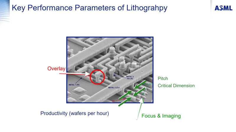
The correct and predictable stacking of, say, sixty different layers is an absolute necessity for a properly functioning chip. This comes together in the concept of overlay – the accuracy with which a lithographic scanner can place billions of structures in a layer on top of the billions of elements in the previous layer. “If you make an overlay error, you have less contact area between features in the layers. As a result, you get more resistance, and when you get more resistance, this results in less speed and more energy consumption,” explains Paarhuis. The better the overlay, the better the yield and chip performance. Paarhuis: “As customers currently split layers into multiple exposures, the overlay performance is even more critical.”

In the past, all layers were exposed in optical scanners with deep ultraviolet (DUV) laser light. Currently, part of these layers is exposed in scanners that use extreme ultraviolet light (EUV). ASML claims its EUV equipment will keep Moore’s Law alive beyond the next decade. This continued scaling puts quite some pressure on the demands for overlay.
In the most advanced fabs, the first layers on bare silicon wafers are structured by EUV lithography. Subsequent layers are printed by DUV immersion scanners, followed by less critical layers that are produced by DUV dry and older-generation machines. The sequence of layering is a relay race where handing over the baton needs attention, especially the step between EUV and DUV (the switch between litho technologies is called cross-matching). “We need to take care of the overlay between a layer that’s exposed on a EUV scanner and a subsequent layer, exposed on a DUV scanner,” says Paarhuis.
The challenge is to match the overlay requirements with the constant customer request for higher productivity. Chip production is, after all, a capital-intensive, high-risk/high-reward game. More wafers per day mean more money for ASML’s customers. The latest NXT:2050i scanners from Veldhoven increase the productivity to 295 wafers per hour (from 275 in the 2000i).
Asked by his audience if it’s possible to have even higher throughputs and, if so, whether customers are willing to sacrifice accuracy for increased productivity, Paarhuis mentions the balancing act ASML engineers are performing daily: “Increasing throughput is quite easy. We have knobs in the scanner to reduce the conditioning time or the time to do the sensor measurements, for example. That will increase the throughput, but with a penalty on the overlay and focus. Customers aren’t interested in that route. They always want a combination of higher productivity and better performance.”
Height map
Making the production of billions of chips with billions of transistors more precise and more productive starts with physics, accurate measurement, analysis and advanced control software. Paarhuis gave some examples of improvements and how they were achieved in the new 2050 scanner.
In physics, the temperature is the parameter that’s most difficult to control. In the new 2050 scanner, both reticles (masks with original patterns for each layer) and wafers (silicon slices to be patterned) are brought to the right temperature before being inserted into the scanner and placed on the reticle stage and wafer stage.
Before a wafer is exposed, it’s measured on one of the two wafer stages. This is done before each exposure because the wafers undergo changes during the patterning and deposition. A level sensor measures the height map in order to bring the wafer in focus while the scanner exposes it below the lens. The height differences can be as large as a thousand nanometers.
On the measurement position, an alignment sensor measures the X and Y locations of special alignment marks. Not only to determine the wafer position to correct for replacement and loading errors of the wafer on the wafer table, but it’s also important to measure the deformation because the wafer gets stressed due to processing in the other steps in the customer fab and during clamping.
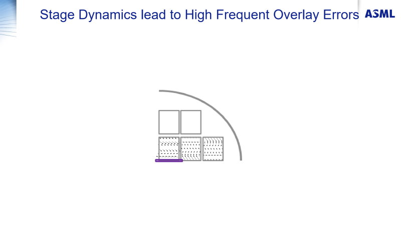
The reticle isn’t exposed in a flash of light, like in a stepper, but in a scanning way, just like a photocopier. For this, the scanner has to hold the reticle stage, move the reticle and clamp and hold the wafer on the wafer table. “Not only to flatten it but also to keep it at the right temperature and hold and move the wafer,” explains Paarhuis. The forces released by these movements are impressive and have to be counterbalanced. However, minor overlay errors caused by these accelerations can still be seen as a nanopattern in the exposures: the errors vary from row to row and from field to field. The 2050 system offers increased stiffness and integrated damping in the wafer stage. Paarhuis: “We were able to reduce the overlay errors by more than a factor of two.”
Optimized routing
To control the movements and forces, it’s necessary to know the exact position of each of the scanner’s components. A central part of the system is the metaframe, a very stable frame, which holds the lens and the grid plates – the yardsticks used by the wafer stage encoders to measure its position. The reticle stage has an encoder to measure its position with respect to the lens. Paarhuis: “This results in a complete measurement system to tie the position of the reticle via the stiffness of the chuck, the encoder, the stiffness of the lens, the grid plates, the encoder of the wafer stage, the stiffness of the wafer stage and the wafer table and the wafer.”
After a wafer enters the scanner, it’s clamped on one of the two wafer tables. Then stage alignment can start – the measurement to exactly locate the wafer. For this, the alignment sensor compares the position of the alignment marks on the wafer to two alignment marks printed on top of the so-called Paris plate, located alongside the wafer position. This provides accurate information about the position and the shape of the wafer.
Next, the scanner measurement system has to accurately position the reticle with respect to the wafer. After the exact position of the wafer with respect to the Paris sensor is determined, there’s a chuck swap: the wafer stage changes its measurement position to the exposure position under the lens. On the exposure side, the scanner starts with the reticle alignment, using seven sensors integrated into the same Paris plate. These seven sensors measure the exposed seven marks from both the top and bottom of each reticle. “With this measurement, we can not only measure the reticle’s position with respect to the plate but also its shape,” explains Paarhuis. “Now the scanner knows the position of the reticle with respect to the Paris plate and because the position of the wafer with respect to that plate is also known, we can start exposing.”
To decrease the overlay errors and simultaneously improve productivity, ASML had to do substantially more wafer alignment measurements in less time. “On the NXT:2000 system, we could measure 28 alignment marks at 275 wafers per hour,” says Paarhuis. “Without extra measures to accelerate the measurements, we ended up locating only 20 alignment marks at 295 wafers per hour.” To do all checks in time, the 2050 team accelerated the alignment scans and measurements of the wafer height map. “We made them faster and were also able to optimize the routing in between the marks.”
As a result, the 2050 system can measure 55 marks at 295 wafers per hour. “This enables a better overlay because we can more accurately measure the shape of the wafer.”

Pellicle bending
A few years ago, ASML found another overlay error contribution. Paarhuis: “Analyzing the data, we discovered a very typical scan-up-scan-down fingerprint.” This distortion pattern is caused by the DUV pellicle and contributes to the errors in DUV-EUV matching.
During exposure, the scanner moves the wafer in a zigzag pattern under the lens. Part of the fields is exposed on the way up and part on the way down. The fields that were scanned up show a specific pattern. “The scan-down fields have the same pattern but flipped,” tells Paarhuis.
These patterns proved to be a result of the pellicle that was deformed by air pressure during its acceleration. The pellicle is a very thin foil that’s stretched in a frame on top of the reticle to protect the mask against dust particles. This DUV-transparent membrane can be as thin as 280 nanometers. During the exposures, while the reticle is scanning on the reticle stage, the pellicle foil deforms due to pressure variations. This causes the light to refract, resulting in a very slight displacement of the image. The error is a function of the foil thickness, the angle at which the pellicle bends and the refraction index of the foil. “On a wafer level, this error is typically 0.5-1 nanometer, so that’s pretty big,” says Paarhuis.

The solution is running a model on the scanner that reduces the pellicle impact. “Using the reticle stage trajectory, we can predict the pellicle bending and use a model to calculate the needed overlay corrections and apply them during exposures.” This works pretty well, says Paarhuis. The model predicts the required correction with an error of only 0.1-0.2 nanometers. “That’s very nice.”
This has resulted in a machine that’s able to keep its DUV-to-DUV overlay errors under a nanometer. Paarhuis even showed champion dedicated chuck overlay data with a total performance of 0.8-0.7 nanometers. “This was done in tests where we typically exposed twelve wafers on the same scanner in three lots. That’s well below the spec of one nanometer.” For DUV-to-EUV cross-matching, the engineering team used six wafers, exposing one layer on the NXT:2050 and one layer on the NXE:3400. ASML’s champion data for the 2050 versus the 3400 measured only 1.2 nanometers.