


With the first shipment of its Luminex platform, building on former Assembleon systems, Kulicke & Soffa underlines its commitment to the equipment market for advanced displays. The company even expects that transfer speeds of 10,000 micro LEDs a second will be able to compete with lithography processes.
Researched at the University of North Dakota, engineered in Eindhoven. That’s the road taken by the first super-high-speed micro-LED assembly machine that was shipped by Kulicke & Soffa, most probably to Samsung. This machine, the Luminex, uses laser-enabled advanced placement (LEAP) to shoot a thousand micro LEDs per second on a substrate. With parallelization, the laser technology even has the promise to gear up to 10,000 placements per second. That speed is expected four years from now and is needed to cost-effectively produce a 4K television screen with 24 million self-emissive LEDs – the equivalent of filling an area the size of a soccer field with euro coins in 40 minutes.
With the technology, obtained through the $25M acquisition of Uniqarta last February, K&S hopes to secure its roadmap and leadership in the back-end equipment market for LED-enabled backlighting. It made a head start there with the Pixalux placement machine for mini LEDs, developed by way of an exclusive IP agreement with US-based Rohinni. The mini variant is in high-volume production since 2019 and is currently revolutionizing the premium LCD market. The Pixalux can position and place up to fifty components a second with an accuracy of 20 micron. At its recent investor meeting, K&S said it had delivered its 100th Pixalux last December. Backlighting with mini LEDs is anticipated to transition to the value-oriented, high-volume display market starting in 2023, the company believes.

Demand is soaring. Market researcher Trendforce expects the amount of 4-inch equivalent wafers with mini and micro LEDs to grow from almost 2 million this year to over 10 million in 2025. By 2024, K&S anticipates micro-LED adoption will accelerate, supporting new self-emissive displays serving specialty markets such as large commercial displays and wearables initially, with the potential to move into higher-volume premium display markets such as smartphones. In that year, the Singapore-based company expects that its LED and advanced display solutions will add 150 million dollars to its revenue.
The current success and future outlook form a mental boost for the K&S engineering crew in Eindhoven. The Pixalux and Luminex systems both have their origins in the pick-and-place platforms of Assembleon, the Philips spin-out that K&S acquired in 2015 for 98 million dollars. This team engineered both the Rohinni and Uniqarta technology and matured the processes to serve the highly demanding back-end semicon market.
Mini-explosion
The Pixalux transfers mini LEDs of about 125 micron mechanically from the substrate to the board. The dies are mounted on tape upside down. A pin mechanically presses the components down onto a printed circuit board into solder paste. K&S expects to improve the speed up to 75 dies per second. Looking at the increasing requirements for high-end displays, however, the mechanical process will eventually run out of steam.
The acquisition of Uniqarta enables K&S to stretch its technology roadmap. The spin-off from the University of North Dakota uses a laser for super-fast transfer from substrate to board. The process resembles the way an inkjet printer works, by evaporating a liquid to shoot a droplet of ink on paper. The LEAP process also uses a micro explosion to transfer micro LEDs to their required position.

To make this happen, a substrate with LEDs has three layers. The first is transparent fused silica or glass offering mechanical strength. The mini-explosion happens in the thin layer on top: the material absorbs the laser puls and evaporates. On top of that, the third layer serves two purposes: it’s an adhesive layer for the LED dies and it’s also capable of containing the mini-explosion.
A substrate with the LEDs upside down is transported above the PCB. The laser beam shoots through the glass layer and the absorbing layer material evaporates, causing a blister that contains the explosion but also presses the component on the substrate. “It doesn’t add debris to the tape,” explained K&S CTO Bob Chylak at the recent investor day. “That’s the genius in this technology. There’s this little micromachine that can transfer the dies very quickly. The laser pulse heats the material for only tens of picoseconds and the die is transferred in microseconds. As opposed to mechanical transfer, this is all positioned by galvo mirrors that can move extremely quickly.”
Complementary
Chylak also shined some more light on the future of the laser equipment. “In the future for micro LEDs where 8K displays can have up to 100 million dies mounted on them, we need much, much faster transfer. So we’re developing the same technology but instead of shooting one die at a time across a gap onto a board, we’re going to shoot many dies simultaneously.”
The Luminex platform also meets the stringent requirements for self-emissive displays. To make these, wafers with tens of thousands of LEDs are produced in wafer fabs. The components are diced and stretched onto a tape. But the dies also have to be sorted and mixed because their wavelengths aren’t uniform. That means dies of the same wavelength need to be put on a newly reconstituted substrate to prevent unwanted color differences. For an RGB display, the LEDs are put on a pitched array module and then placed on the substrate.
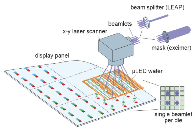
“The Pixalux today can do the final placement onto the substrate but doesn’t do the sorting or the repitching,” Chylak explains. “The Luminex can do sorting, repitching and the final placement with its better accuracy and laser transfer. It opens up RGB applications for both mini and micro LED.” The automatic replacement of defective dies was also developed by Uniqarta. Contrary to the mechanical transfer technology used in the Pixalux, K&S owns all IP of the LEAP technology.
K&S believes the rapid transfer technology will even be able to compete with lithography. In an interview with LEDinside, Chan Pin Chong, responsible for products and solutions at K&S, said that micro LED could replace expensive pre-fabricated photomasks or beam scanning methods. LEDinside notes that micro-LED lithography technology has demonstrated under 5 µm resolution and could be scaled down even more to sub-micron.
While the Pixalux serves the market for backlighting applications, the Luminex serves both backlighting and self-emissive displays. However, CTO Chylak stresses that the latter won’t replace the former. Revenue from both machines will continue to increase in a market expected to grow at an average of 66 percent in the coming years. Chylak: “Mini and micro LED are complementary and they’ll coexist in the future.”
Main picture credit: Bernard Hermant on Unsplash