


As a young research scientist, he created the Netherlands’ first EUV image. It was the prelude to a partnership with ASML and other companies that has already lasted a quarter of a century. Yet Fred Bijkerk remains first and foremost a scientist.
‘It was just like with the printing press. That was also invented multiple times,’ says Fred Bijkerk, a professor of XUV optics at the University of Twente and the man who in 1990 projected the first EUV images in the Netherlands. He was unaware of the work being done by Kinoshita on the other side of the world. ‘The experiments were carried out largely independently of one another, but the Japanese were clearly the first: all the honour belongs to them,’ Bijkerk says.
Either way, the name Bijkerk will always be linked with EUV sources and optics. The technology is the common thread that runs through his career. He wrote his master’s thesis on the spectroscopy of laser plasmas and his doctoral dissertation on using laser plasma EUV sources in lithographic applications. Since 1990 he has led the Laser Plasma and XUV Optics group at the FOM Institute for Plasma Physics in Rijnhuizen, which moved in 2013 to the Mesa+ Institute for Nanotechnology at the University of Twente.
In addition to his scientific research, Bijkerk coordinates the XUV Optics focus group, through which he works with ASML, Zeiss and other companies to further refine industrial EUV optics – not only for photolithography, but also for other applications. For example, the x-ray analysis equipment manufacturer Panalytical is also a member of the group. Similar optical elements are used for that application.

How did you come to build a setup that enabled EUV lithography to be used in practical applications?

Bijkerk: ‘Out of curiosity. And because we had the technological capabilities at that time. We could already make EUV mirrors with good reflectance because we were researching spectroscopy in that wavelength range. We wanted to study a metallic phase of silicon that briefly occurs after you’ve injected a great deal of energy into the material in a short time. For that, we needed light at a wavelength of 12.5 nanometres. That meant we had to create a light source – we used a laser plasma, just like ASML still does in EUV scanners – and a mirror to filter the desired wavelength out of a broader spectrum. And with that, we had the most important ingredients for photo lithography at our disposal.’
‘I’ve always enjoyed the practical side of science. You see that in a lot of scientists, and certainly in my doctoral students. Publishing is of course one of life’s main objectives for our kind, but it’s also a real kick when society or industry takes our work and runs with it. The essence of our work remains fundamental research at the highest level, but practical applications give it added meaning.’
The semiconductor industry is currently working at a wavelength of 13.5 nanometres; you used 12.5 nanometres. Did you choose wrong at the time?
‘The industry makes its own choice about the wavelength it wants to use. We scientists simply present the facts. When we started the project, we thought we’d get much further with 12.5-nanometre palladium-carbon mirrors. But once the industry had made its choice, there wasn’t much of a future for 12.5 nanometres, and we switched to 13.5 nanometres.’
‘Funnily enough, 13.5 nanometres isn’t optimal, either; 14.4 nanometres is better. The peak reflectance value is a little lower there, but the bandwidth is broader. If you’re lining up multiple mirrors one after another, the bandwidth is more important than the reflectance. I think that at a given point, a choice had to be made, and 13.5 nanometres had the most support in the industry at that time.’
When did you approach industrial partners with your ideas?
‘I went to Steef Wittekoek, at that time ASML’s chief scientist, at a pretty early stage. He was very critical, but he became convinced that our work had potential for his company. At that time, STW was running a programme that you could only apply for if industry was interested. With Wittekoek’s support, I applied for – and received – funding to demonstrate that EUV lithography is possible. It was proof of principle.’
Tell us more about that experiment.
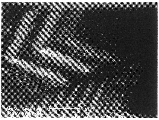
‘We imaged sub-microstructures, but still far from the limit for that wavelength. It was a kind of feeling things out, an exploration of everything that’s involved. Remember, no one had much experience in creating images using light at that wavelength.’
‘For our light source, we used a metal disk, with a laser that vaporized a bit of material into a plasma, which emits light as it cools. Tantalum worked well, and so did iron. We were able to get a half watt of power pretty quickly, which is a surprisingly large amount for such a primitive approach. That promised the ability to scale up.’
‘We also had to deal with undesirable side effects and difficulties, such as material that precipitated onto the mirrors. And we didn’t yet have an EUV-specific resist, either. Colleagues at TU Delft more or less lucked into making one for us. These are issues that have turned out to be very relevant for industry, and at the same time have given rise to extremely interesting new scientific questions.’
Such as?
‘The effects of light on a mirror. We’ve learned to make mirrors that reflect almost up to the theoretical maximum, but light initiates all kinds of ancillary processes, such as the interdiffusion of materials. Atoms start to migrate, which makes the originally sharp, almost black-and-white contact surfaces blend a little, and the mirror’s performance suffers.’
‘For industry, this intermixing process is very detrimental, because it limits the mirrors’ lifespan. But combating that diffusion is also a scientific problem. We solved it by placing a diffusion barrier between the layers. If you do it right, you can even improve optical performance. Now we’re scouring the periodic table to find the best material to use.’
So even today your group is still trying to improve reflectance?
‘Our record is 70.3 per cent with a theoretical maximum of 74 per cent. We won’t achieve the maximum, because it assumes that atoms have no dimensions. But we will achieve 71 per cent. For industry, every extra per cent is welcome. There are multiple mirrors in a system, and light is lost at every mirror – the loss grows exponentially. So even a small improvement in an individual mirror’s performance means a significant improvement in the system’s performance. That’s important for future scanners, which may need to contain even more mirrors.’
Are you proud? You provided the impetus for a technology that advances Moore’s Law and thus has an enormous impact on individuals and societies.
‘I can only lay claim to a very tiny piece of that development. Hundreds of people have worked on it, and I don’t think anyone has the idea he was indispensable. And as a scientist, I don’t focus primarily on an idea’s application. I admire those people who had the courage to industrialize EUV lithography, and for me that process has been a source of inspiration – and it still is. Listening to others, hearing the questions with which your colleagues and industry are wrestling; you help your field move forward when you do that. You achieve more doing that than by sequestering yourself in your own lab.’