
Why ASML isn’t worried about Applied’s pattern-shaping tool
ASML’s stock took a bit of a tumble on the last day of February when Applied Materials announced what some investors apparently considered to be a threat to EUV scanner sales. Those fears are overblown. Even if Applied’s “pattern-shaping technology” works as well as advertised, the Veldhoven-based equipment manufacturer stands to gain from the widespread adoption of the Centura Sculpta system.
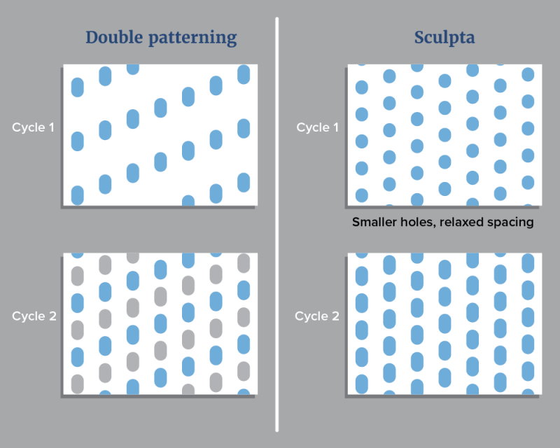
The Sculpta is a selective etch tool designed to asymmetrically remove material. By moving a plasma beam at a configurable angle and speed across a wafer, the chemically reactive species nibble away at the sidewalls of existing features, thus changing their shapes. Holes, for example, can be elongated into ellipsoids.

Although this technique can’t enhance patterning resolution, it can enable the creation of denser patterns without having to add another lithographic cycle, ie applying double patterning. Consider the pattern of holes mentioned above. The minimum diameter of the holes is dictated by the specs, but the closer together they’re spaced, the more of them fit into a given area. The spacing is lithographically constrained, however. Tight spacing demands a two-step procedure, with two sets of holes being patterned sequentially.
The Sculpta, Applied showed in a press presentation, can replace the second cycle of deposition, lithography, etching and other processes with fewer steps. First, smaller but more densely packed holes are patterned in a standard lithographic procedure. Next, the Sculpta tool is used to enlarge the holes, putting them closer together than would have been possible with a single patterning step.
Unique
Applied presented the Sculpta as a way to reduce the need for EUV lithography in certain situations. The press material focuses on two double-patterning use cases, one of which is outlined above, but there may be others as well. At any rate, it’s clear that the Sculpta isn’t a replacement for lithography. It’s complementary.
Even so, Applied claims significant cost savings on the presented double-patterning use cases, partially by reducing complexity. For every EUV double-patterning sequence it replaces, the Sculpta can save 50 dollars per wafer or 250 million dollars per 100k wafer starts per month. Furthermore, Applied says the technique is ready for mass deployment, having been in development for six years with leading customers. Intel and Samsung had nice things to say about it.
Analysts disagree on the potential impact of the Sculpta. Robert Maire of Semiconductor Advisors isn’t impressed, calling it “just another etch tool,” one that mimics a product of Tokyo Electron no less. “To suggest that the Sculpta is a replacement for double-patterning EUV is a stretch, as it only serves as a replacement in certain circumstances and far from all. So to suggest this will have some sort of significant impact, like eliminating double patterning, or EUV usage is also a long stretch.”
Scotten Jones of IC Knowledge has more faith, calling the Sculpta a “useful addition to the lithographer’s tool set.” He notes throughput will be a major factor in terms of how much cost it can save, “but it would have to be incredibly slow for the Sculpta tool not to be a much less expensive option than an EUV litho-etch loop.”
Dylan Patel and colleagues from Semianalysis are downright enthusiastic, writing that the Sculpta will “redefine the lithography and patterning market,” pointing out that “the shaping use case is clearly unique.” Based on an analysis involving the tool’s throughput, cycle time, cost, shipment estimates and revenue estimates from customers, Semianalysis arrives at a 4.5-billion-dollar reduction in EUV demand in the future. Only the market research firm’s paying customers know when that will be, but it could be very far out. Still, for reference, ASML’s EUV system sales revenue amounted to 7 billion dollars last year, an increase of 13 percent YoY.
Commonplace
For argument’s sake, let’s assume the Sculpta works pretty well. Chip manufacturers already apply EUV double patterning in production, and going down the nodes, they’ll have an increasing need for it, even as high-NA enters the scene. Eventually, high-NA double patterning will be commonplace, too. This drives demand for ASML’s tools. Clearly, the Sculpta could take away some of that demand.
But the Sculpta will also generate new demand. In this phase of Moore’s Law, in which dimensional scaling has slowed down and will continue to do so, anything that helps reduce cost helps to keep the industry growing. “We welcome any enabler of process improvement. Over the last few years, we’ve worked with many partners on resist, mask and etch technologies for EUV. Improved resist sensitivity, imaging contrast, and so on, have all resulted in significant gains in productivity or imaging performance. In turn, those gains resulted in major cost savings for our customers in the EUV ramp,” an ASML spokesperson answered a comment request of Bits&Chips. “In the coming months, we’ll work whenever needed with customers to see what benefit [the Sculpta] brings.”
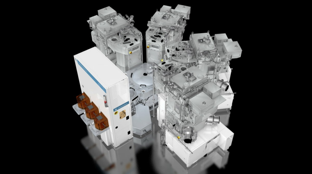
Main picture credit: Applied Materials


