


IBM has just popped the lid on 2nm technology. As a research partner, it might help Intel catch up with TSMC.
IBM’s unveiling of the world’s first 2nm-node chip might be just what the doctor ordered for Intel. Having embarked on a mission to regain leadership in the semiconductor industry, the processor maker desperately needs to catch up to TSMC in process technology. Thanks to the recently announced research collaboration with Big Blue, the 2nm chip could help to make up ground.
IBM bowed out of semiconductor manufacturing in 2014, paying Globalfoundries 1.5 billion dollars to take the ailing chipmaking unit off its hands. The company, however, didn’t stop developing advanced semiconductor technologies. On the contrary: partnering with public and private parties at its R&D facilities in Albany, New York, it continues to work at the forefront of semiconductor innovation. Samsung has been a long-standing partner in this ecosystem, while former rival Intel joined last March.
Whether Intel will actually use (elements of) IBM’s 2nm technology is unclear. “We expect all our partners to benefit from this innovation,” was all that Mukesh Khare, IBM’s VP of Hybrid Cloud Research, would say about that. There’s no doubt Intel has been working on similar technology, but since it hasn’t announced a full-blown chip containing it, despite needing all the good PR it can get right now, one might speculate that IBM was ahead and therefore might be able to accelerate Intel’s development process.
In the end, however, what matters most is how long it takes for the test chip to be developed into mass-producible technology, and how it will stack up against TSMC’s offerings by then. According to IBM, the chip will be foundry-ready by late 2024. Reportedly, TSMC’s 2nm node will enter mass production in 2024 as well.

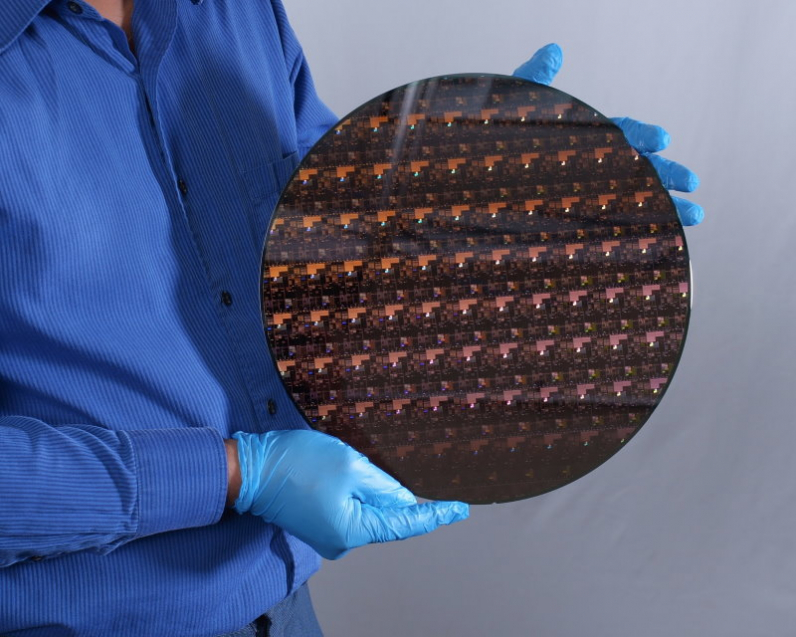
Fingernail
IBM’s new chip represents the next step in the evolution of CMOS. As dimensions of transistors shrink, the proximity between the drain and the source lessens the gate electrode’s ability to control the flow of current in the channel. That’s why leading-edge chipmakers in the early 2010s moved to the FinFET architecture, in which the channel is raised to a 3D fin structure with a gate draped over it on three sides. Like its planar predecessor, however, the FinFET was always going to run out of steam at some point, necessitating complete envelopment of the channel.
Naturally, all leading-edge chipmakers have been working on these gate all-around (GAA) transistors, using either nanowires or (stacks of) nanosheets as the channel. In fact, Samsung is planning to move its nanosheet 3nm process to production next year. TSMC is initially sticking with FinFETs at 3nm but is preparing for a transition to the nanosheet GAA transistors as well. Intel has also shown work on what it calls nanowire/nanoribbon transistors and has stated that it will use them in high-volume production before 2025.

It’s therefore no surprise that IBM’s 2nm chip, too, features the GAA architecture. Each transistor consists of a 75 nanometer high stack of three nanosheet layers, each 40 nanometer wide and 5 nanometer high. The pitch is 44 nanometer and the gate length 12 nanometer. Big Blue claims that 50 billion of them will fit on a fingernail (150 mm2) to create chips that will achieve 45 percent higher performance or 75 percent lower energy consumption than today’s 7nm node chips.
EUV
IBM highlighted several key innovations that enable the miniaturization effort. One is the use of bottom dielectric isolation, which entails introduction of a dielectric layer underneath both the source-drain and gate regions. This prevents current running through the sheets leaking into the wafer, improving power and performance.

Another novelty is a multi-threshold voltage control scheme that allows for tuning the transistors to specific applications. The threshold voltage is the minimum voltage needed to create a conducting channel between source and drain – in other words, the minimum voltage to turn a transistor ‘on.’ Low threshold voltages allow for quick switching, but at the cost of higher current leakage. Transistors with multiple threshold voltages can be optimized for their intended application, ie pure performance in high-performance computing or much more geared towards low power consumption in mobile processors.
And, finally, IBM was the first to use extreme ultraviolet lithography (EUV) for front-end of line (FEOL) processes. FEOL is the first part of IC fabrication, where transistors and other components are made. According to IBM, all critical layers in the 2nm chip can still be patterned with a single EUV exposure step. Until now, EUV has only been used for wiring and interconnects.