


ASML’s senior vice president technology Jos Benschop recently revealed how the EUV ecosystem centered around his company’s lithography scanners will continue to shrink chip structures for the decade to come.
Going from i-line bulbs in the mid-80s to EUV light sources today, the resolution required to pattern the world’s leading-edge chips has gone down by two orders of magnitude. For a while now, ASML has been saying that this historic trend can continue for at least another decade. But other than putting high-NA EUV lithography on the roadmap, it hasn’t gone into much detail on how this feat will be accomplished. Speaking at the SPIE Advanced Lithography online conference recently, ASML’s senior vice president technology Jos Benschop lifted the curtain.
The issue that his audience probably was most eager to hear about is stochastics. Indeed, Benschop himself referred to it as “the elephant in the room.” Stochastic errors, which are random variations in patterning, have been plaguing EUV lithography right from the start. It has been a hotly debated subject, particularly at specialist forums such as the SPIE AL conference.
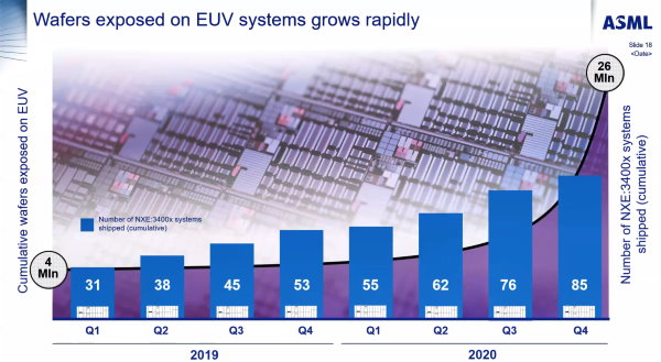
And it still is. Even though stochastics clearly hasn’t been a showstopper for commercial implementation – the EUV counter reached 26 million exposed wafers by the end of last year – things get progressively more challenging as chip structures keep shrinking. Introduction of high-NA EUV lithography is part of the solution, but will not make the problem disappear.
Secondary
Stochastic effects manifest themselves as random, non-repeating and isolated defects in the printed pattern. The result can be locally broken lines, missing or ‘kissing’ (merging) contacts or microbridges that link structures that shouldn’t be connected, among other things. Any one of these defects could ruin an entire chip. Without countermeasures, yields would suffer detrimentally as the margins of error shrink along with chip features.
These printing failures arise partly from not having enough photons. EUV photons are relatively high in energy, so the same amount of energy can create fewer 13.5-nanometer photons than, say, 193-nanometer photons even if they would be generated with the same efficiency. Because every spot on a wafer gets hit by photons according to a random distribution pattern, the lower the number of photons, the more random fluctuations. Increasing exposure time will increase the number of photons that land on a spot but will also decrease throughput and hence increase patterning costs.
Clearly, more powerful EUV light sources, producing more photons, will help. Benschop showed a source power roadmap that goes up to 800 watts. It will take years, however, before that number is reached. For comparison, chipmakers are currently using 250-watt sources. In research, ASML recently demonstrated 420-watt power sustained for several hours and 500 watts in peak bursts.
An equally important factor in stochastics is the resist. Ideally, a resist would be a continuum. In reality, it’s ‘broken up’ in molecules, which are by definition discrete entities – ones that will never spread completely evenly across a surface no matter how hard you try. Additionally, the absorption of energy-rich EUV photons can set off all sorts of secondary chemical reactions in the resist.
ASML and chipmakers are counting on resist makers to come up with resist formulations that cram more molecules in a ‘pixel’ and that absorb more photons while suppressing undesirable processes.
Holistic view
So, there are roadmaps for source power and resist characteristics. Will that be enough to keep stochastics in check without escalating light doses to painful levels? No, Benschop showed. Additional measures will be required.
In his presentation, Benschop zoomed in on an issue with a large stochastic component called edge-placement error (EPE), which is basically the margin of error for positioning IC features relative to each other. It’s “perhaps the most decisive factor in the future of shrinking,” he said.
Currently, at the 7nm node, about 40 percent of the EPE budget is down to stochastics. The other two major contributing factors are the overlay (also 40 percent) and the optical proximity correction settings (OPC, 20 percent).
There’s room for improvement in the OPC, Benschop showed: deep learning techniques enable an OPC accuracy improvement of up to 77 percent. This gives a little more breathing room for stochastic errors.
Then there’s another factor contributing to stochastics, which hasn’t been mentioned yet: contrast. Contrast is improved by migrating to high-NA and reducing the k1 factor, a collection of everything that increases resolution other than increasing NA and reducing wavelength (remember: maximum resolution = k1 * (NA/λ).
An important k1-reducing measure will be switching to a more advanced mask design called an attenuated phase-shift mask. Another will be extending ASML’s holistic lithography suite. By having metrology, computational modeling and advanced scanners controls working together, errors in the patterning process can be detected and corrected, often in real time. As an example, Benschop highlighted carefully controlling how light hits the reticle, ie shaping the light beam into the optimal ‘pupil shape’ (which can range from simple spots to complex patterns) for a given pattern.

Even with all these improvements in place – higher source power, moving to high NA, better resists and k1 reductions including OPC improvement – it’s not enough to get stochastics under control while maintaining cost-effective throughput. That’s why ASML has little choice but allowing for a larger percentage of the EPE budget to come from stochastics: up to 60 percent in the future. The difference will have to be made up by improving OPC and overlay.
“We’ll be even more aggressive on the overlay roadmap,” Benschop said. “We plan to improve overlay faster than the resolution. This way, we manage to maintain almost constant productivity moving into the future. Assuming the aggressive source roadmap, high-NA and low k1 as shared. This holistic view of scanner, mask, resist, computation, as well as metrology coming together, will bring us increased resolution at acceptable productivity moving forward into the future.”
This article was written with contributions from René Raaijmakers