


ASML closed the last quarter with unexpectedly high sales in DUV systems and upgrades. In all of 2020, the orders totaled 7.3 billion euros. This shows that the chip lithography workhorse is still in a rock-solid position in the coming years.
In recent years, lithography with extreme ultraviolet light (EUV) attracted almost all the attention. The technology has captured the imagination. If only because ASML has so far been the sole supplier. EUV lithography now defines the performance of the most advanced systems on Earth, from Samsung’s Galaxy and Apple’s iPhone to servers in data centers.
With that, EUV is also highly strategic. The world’s most successful semiconductor companies use it to make their microprocessors and AI chips. Companies like Apple, Nvidia and Qualcomm have their products made by parties that have the knowledge and the courage to do so – setting up an EUV wafer fab is extremely difficult and requires deep pockets. So far, only Intel, Samsung and TSMC are playing in this league.
In addition to this trio, SK Hynix is about to invest in EUV. Only Chinese SMIC is known to be an EUV wannahave. However, the governments of the US and the Netherlands are blocking EUV machine deliveries to China – how strategic can it get?
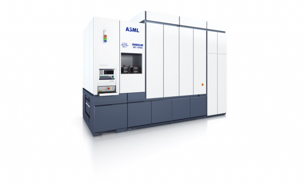
Meanwhile, the focus on lithography with deep ultraviolet light (DUV) is somewhat pushed to the background. Unjustifiably so, because DUV is profiting from expanding markets. Moreover, every order for an EUV machine also means orders in DUV. The figures show that DUV is a healthy business. ASML sold 5.4 billion euros worth of DUV systems in 2020, compared to 4.4 billion in EUV machines. That 5.4 billion consisted of nearly 4 billion euros in 68 immersion systems, the most advanced DUV machines.

The DUV playing field is less monotonous. ASML still has a motley crew of customers in that segment, but it faces some competition – albeit modest – in both immersion and dry segments: Nikon in ‘wet’ immersion and Canon in the low-cost segment of dry machines.
The high-end game seems to be over. Canon has never had the guts nor the ambition to make a difference in EUV; Nikon lacks the means. Whereas ASML has branches all over the world to supervise the installation of new systems, Nikon was seriously hampered as its engineers were slowed down by Covid restrictions. In April, May and June, it only sold three semiconductor lithography systems, compared to seven in the same quarter in 2019. In the flat panel litho market (where ASML isn’t active), it’s experiencing the same setback. The decline in camera sales is also contributing to its losses.
Both Japanese competitors still earn a reasonable living from service and maintenance. Nikon, for example, has three thousand systems mashing chips every day. In Veldhoven, however, they’ll view this first and foremost as a thing of past glory.
ASML not only has a monopoly in EUV, but it also dominates immersion lithography – the DUV segment with high prices and margins. Nikon expects to sell only seven of these systems in its 2021 fiscal year (March 2020 to March 2021). ASML did 68 in 2020. Canon has long been out of this game. It did make a valiant effort to catch up in 2005 and 2006, but it sold only three systems in 2008 and 2009. In the two years that followed, shipments remained at zero, after which it forfeited the fight.

Within the DUV portfolio, the price differences are considerably larger. The most expensive DUV immersion systems use 193 nm light from an ArF laser and project their patterns through a water layer between lens and wafer. These cost around 60 million euros. The dry ArF systems fall into an entirely different price range, at around 20 million euros, while KrF machines cost 10 million euros. I-line machines do not fall within the DUV category. They image patterns with the spectral i-line from a mercury lamp. For that type of system, ASML charges around 5 million euros.
Investment appetite
Ron Kool, leading the DUV business at ASML, points out that a transition to EUV will only boost demand for DUV. Chip manufacturers deploy EUV in the early stages of chip fabrication to apply the smallest structures: the transistors and also the smallest vias (the contacts that connect source, gate and drain to the complex interconnect layers) and possibly a connect layer. Up next are ArF immersion scanners, then dry ArF systems, and then machines that still use the ‘old’ KrF and i-line. All this to build the chip’s stack, the sum of sometimes more than a hundred interconnection layers. Kool: “It’s about the whole stack. This stack is only growing and the number of critical layers is only increasing.” Thus, as EUV grows, DUV grows just as fast.
“DUV does the bulk of the layers and will continue to do so for some time,” underlined ASML CFO Roger Dassen at the presentation of the annual results to analysts. “That’s also why we still have extensive R&D programs for DUV. In general, DUV will continue to represent a larger share of our business in the future. Not only for memory but also in all kinds of applications and markets that use 90, 65, 45 and 28 nanometers. All are growing if you count the number of wafers. We underestimated that trend a few years ago.”
Nikon says that for 7nm and 5nm chips, you don’t need EUV, but that still seems to be mostly a marketing message born out of necessity. In theory, the message is true. 7nm and even 5nm details can also be produced if you use multiple immersion exposures for one layer. So there are some bells and whistles involved, but in principle, you can then form the structures with DUV that you also achieve with EUV – even if DUV is limited per single exposure to details of 32 nm. That multipatterning technology does come at a cost in terms of yield. “Our customers see that the electrical properties with single exposures with EUV are better compared to multiple patterning,” says Kool. “A higher yield per wafer also means cost savings, and as you start to scale, the whole cost structure at some point falls more favorably to EUV.”
The parameters, the precision calculation and the tipping point may differ for each manufacturer. What’s clear, however, is that the market is still shifting. After the big three logic giants, memory manufacturers are now also looking at EUV. Samsung already uses EUV for its DRAM memories and speaks highly of the quality of the DRAMs it makes with this technology. TSMC also uses it to make fast GDDR DRAMs for Rambus, but that’s only a fraction of its total production.
The rebound in the memory market is giving players an investment appetite. CEO Peter Wennink expects ASML’s revenue for memory manufacturing to rise 20 percent this year, to 3.3 billion euros. “Although DRAM today mainly uses DUV, we still expect an increase in our EUV deliveries to DRAM customers in the coming years.” This week, it became clear that Hynix will make the move to EUV. The Korean company announced that it has finished building a new 3.5 billion dollar DRAM plant. The building will be equipped with EUV pedestals, the foundations with connections needed to carry the double-decker-sized machines from Veldhoven. Hynix says it can start EUV production in the second half of this year.

Extra push
The move from DUV to EUV is a difficult consideration. Immersion machines are more than half the cost of EUV systems, but they’re much more reliable and productive. ASML and Nikon are in a neck-and-neck race when it comes to speed in immersion. Until recently, their fastest systems were doing 275 wafers per hour. ASML’s new Twinscan NXT:2050i trumps that with 295 wafers per hour.
ASML’s fastest EUV system achieves 170 wafers per hour and has a much shorter mean time between interruptions. Mastering the manufacturing technology is extremely difficult. It took pioneers Intel, Samsung and TSMC as much as six years to do so. At the start of the EUV introduction, that seemed like a big gamble. Kool: “But look where TSMC is now. That investment has certainly not done them any harm.” A lot of manufacturers either didn’t dare or thought it was too expensive to make the move so early. It’s significant that Globalfoundries announced with great fanfare at the beginning of 2018 that it would start EUV production but canceled the whole project less than six months later.
The move to EUV will certainly get an extra push if ASML succeeds in making more reliable, productive machines. It expects to bring an EUV scanner (the Twinscan NXE:3600D) to the market this year that’s more productive and reliable. This does, however, come with a higher price tag.
ASML also invests substantially in high-end DUV development. The 2050i it delivered in the last quarter of 2020 is a new version of the NXT platform boasting improvements in many areas: reticle stage, wafer stage and projection lens. It has a higher throughput and provides more grip on the overlay. ASML subsidiary Cymer developed a new laser for the system that makes the smallest lines less frayed, all to increase the yield for chipmakers who want to stay with DUV in the high-end anyway. By doing so, ASML is enabling them to get even more out of the technology they’ve been familiar with for years.
According to Kool, “Customers switch to EUV if they can’t shrink further with DUV or if it has a clear cost advantage. They make their choice based on yield, cost and lead time. I think EUV is also inevitable for memory manufacturers if they want to stay competitive. In memories, cost is definitely a factor. EUV has more of a cost advantage there when you look at specific resolutions. Memory manufacturers can also scale with DUV, but at a certain point, multipatterning becomes very complicated. The overlay must be excellent, but even then, the properties of EUV chips are better.”
3D NAND fabrication is currently only being addressed by DUV, but in the DRAM market, manufacturers are starting to switch. Although, of course, the same law applies here as in logic: DUV continues to expose a large number of layers.

Firmer competition
In growing markets, all players usually benefit. Canon, which offers neither EUV nor immersion systems, expects to sell 134 dry systems this year (ArF, KrF and i-line), up from 84 and 122 in 2019 and 2020, respectively. For its entire chip lithography business, the Japanese company foresees sales to increase 36 percent this year. The growing numbers show the resilience of the Japanese in the dry segment. In comparison, ASML sold 159 machines in the ArF dry, KrF and i-line segments last year.
ASML has announced a dry KrF scanner that can handle over 300 wafers per hour but will only start delivering the first systems in the second half of 2022. With this machine, it claims to have a better proposition than Canon, which has a KrF scanner with a throughput of 230 wafers per hour. ASML says it offers a lower cost per wafer and smaller floor space – an important parameter in advanced chip factories.
You could also say, ASML hasn’t been paying attention, or perhaps more plausibly, Veldhoven has other priorities. The fastest KrF scanner ASML has on its website does 240 wafers per hour. Did ASML offer room for Canon here? “I won’t deny that there’s firmer competition in this segment,” states Kool. “But you have to look at it in context. ASML has always been good at performance. Overlay is a hugely important parameter for yield. That’s where we have a head start and we haven’t been idle. Our XT platform has about reached its maximum capacity at 250 wafers per hour. That’s why we’re now going to migrate all dry litho systems to the NXT platform. It’s all about timing. You want to be ready when customers need it. With NXT, the focus has always been on functionality, on having the best performing machine in terms of accuracy. Now, we’re also going to deploy NXT in a segment where cost and price play a bigger role. For customers, it’s a very simple calculation. They look at wafers per hour and divide that by the cost of the system. NXT outperforms XT there, but it’s a challenge to make that step.”