


Grueling work with Intel cemented the company’s position in the atomic layer deposition market, but the emergence of more ALD semiconductor applications was required for that investment to really pay off. The story of why ASM International is doing so well these days.
ASM International is on a roll. While the semiconductor industry has been experiencing a cold spell since mid to late 2018, the Almere-based semiconductor equipment maker has been posting one quarterly sales growth after the other. Last July, front-end sales even reached an all-time record – and the orders keep pouring in. Many of those are for ASMI’s atomic layer deposition (ALD) systems, which at the moment are its best selling product line, CEO Chuck del Prado noted in a conference call with investors, though he added demand is generally healthy in other businesses as well.
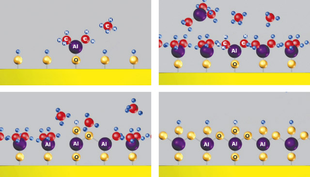
ASMI is currently tasting the fruits of perseverance. The company got into the ALD game as early as the late nineties, when the semiconductor industry still did not have a need for it. After buying the Finnish ALD pioneer Microchemistry in 1999, ASMI worked with Intel for years to replace silicon oxide as the gate dielectric.
For decades, silicon’s natural oxide had been a very convenient isolating layer between the gate electrode and the transistor channel, but as its film got thinner throughout the years – a necessity to increase gate capacitance – it also started ‘leaking’ more and more current. It was clear at some point a new material would be required, one that could do silicon oxide’s job as a thinner film while at the same time leaking less current. Being capable of depositing films literally atomic layer by atomic layer, ALD seemed a perfect technique to create these so-called high-k structures.
It is, as it turned out – though it took years of development to get everything right. Intel demonstrated the first processors with ALD layers in 2007, which hit the market around 2009. It cannot be called the commercial introduction of ALD’d high-k-materials in the semiconductor industry, as the memory industry had been using high-k for a few years already, but it certainly was a first for the advanced logic chips. In hindsight, this achievement cemented ASMI’s position in that segment.

Good times
It took several more years, however, before ASMI’s arduous work started paying off handsomely. At the time, in fact, several activist investors didn’t see the potential. All they saw was a long-time ailing front-end business that dragged down the price of the company’s stock: back-end equipment manufacturer ASM Pacific Technology, in which ASMI controlled a majority stake, was worth more without the front-end activities. The investors therefore aggressively pushed for the front end to be spun out, which ASMI’s management vehemently opposed.
The sordid fight was briefly interrupted by a bid from Applied Materials, acknowledging ASMI’s role in the major process technology transition, but the start of the financial crisis in 2008 quickly put an end to the negotiations. The case for splitting up ASMI was then taken all the way to the Supreme Court, with management eventually prevailing.
Around the same time, additional ALD applications emerged in the semiconductor industry. As DUV lithography scanners had reached their resolution limits and EUV lithography was far from ready for commercial introduction, chipmakers had to resort to patterning a single chip layer in two or more steps. Like adopting the new gate oxide, this multi-patterning technique required deposition of delicate and conformal thin films to ‘split’ a single structure into two structures.
Thus, multi-patterning is an important business driver for ALD equipment. For high-k, basically, only one ALD layer is needed, while multi-patterning is applied to an increasing number of chip layers as the industry progresses through the nodes. Intel’s 10nm chips – the production of which is currently being ramped up – contain a lot more double-patterned layers than the 14nm generation. The same goes for the 5nm ICs that foundries are starting to manufacture. The adoption of EUV has not and will not put a stop to multi-patterning, as the latter often still is the most economical patterning option for all but the most complex layers.
“The current most advanced nodes – 10nm in logic and 5nm in foundry – have been a major inflection in terms of ALD needs. Driven by further miniaturization, new materials and new, more complex device architectures on the industry’s roadmap, the need for additional ALD applications at future nodes will only further increase. This will support continuing healthy growth in these segments of the ALD market over the longer term,” Del Prado told investors.
Simultaneously, new semiconductor ALD applications emerged in memory, such as patterning capacitor dielectrics and for 3D NAND flash. ASMI supplies memory makers as well, but currently, this market segment is going through a deep downturn and only an occasional order contributes to ASMI’s sales increases.
Nonetheless, with logic driving demand for the time being and memory eventually recovering, it seems ASMI has plenty of opportunities to keep the good times rolling. Which is not to say it will be easy going. The semiconductor ALD market is heating up as ambitious start-ups are entering an already quite crowded arena. Tellingly, Applied Materials recently also expanded its presence by buying Kokusai Electric hours after ASMI settled patent litigation issues with the Japanese company.
Looks like ASMI is set up for yet another very interesting decade.