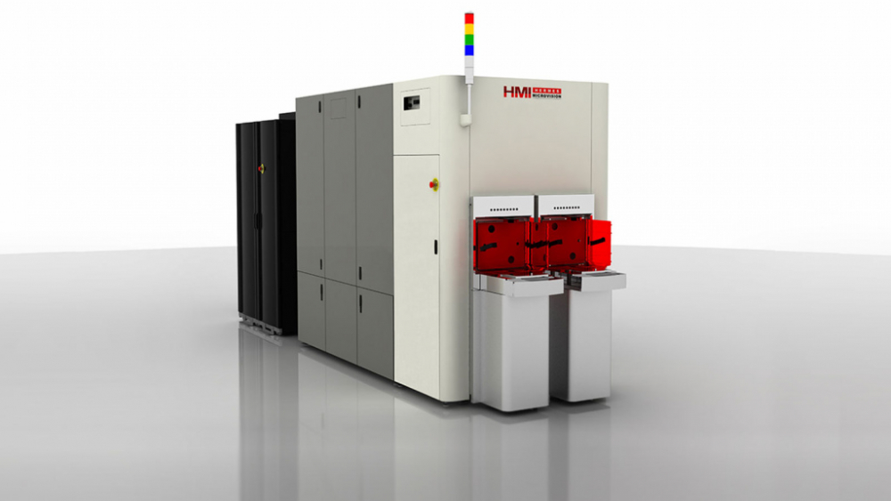
After a complication in IP sharing, ASML was forced to start over developing a multi-beam e-beam metrology tool. As a result, the launch of the system was delayed by a year.
When ASML acquired US-Taiwanese metrology specialist Hermes Microvision (HMI) in 2016, the Veldhoven company had a clear vision for its e-beam inspection tools: integration in the holistic lithography suite. This assortment of computational and metrology techniques in and around ASML’s scanners helps to make sure that chip patterns are printed correctly on the wafer. Over the past few years, the additional control has become a must-have in chip manufacturing at the leading edge.
The addition of e-beam to the exclusively optical inspection methods in ASML’s suite makes sense. Much like lithography is limited by wavelength in what size features it can print, the minimum detectable defect size is capped for optical metrology. At the same time, as chip features get downscaled, the margins of error shrink and increasingly small defects can ruin entire chips. So helping chipmakers to find and analyze them thus presented ASML with a nice revenue-increasing opportunity. Electrons can help do that because it’s easier to produce low-wavelength electrons than photons.
E-beam is notoriously slow, however. A single electron beam takes ages to trace the entire surface of a wafer. Unsurprisingly, HMI’s tools were originally used for process qualification and calibration.
ASML and HMI figured that, together, they can speed up e-beam inspection significantly: when the information obtained by holistic lithography is used to direct the e-beam to ‘hot spots’ on the wafer, the search area is dramatically narrowed. So there’s a two-way synergy happening here: e-beam inspection expands the holistic litho suite and the holistic litho speeds up e-beam inspection. All the more reason why it made sense for ASML to acquire HMI.
Real-time feedback
The integration of e-beam into the holistic litho suite still leaves a lot to be desired as far as speed is concerned. The obvious solution: multi-beam tools. This is another justification for the acquisition: ASML’s deep pockets to fund and accelerate the R&D effort to increase the number of beams.
HMI and ASML have been working on their first multi-beam tool for a couple of years now, featuring nine beams in a 3×3 configuration. It’s mainly intended for process development R&D, but it could also be used in production applications whenever optical inspection just doesn’t cut it.
The question is: where are these tools? The first ones were supposed to ship at the beginning of last year but weren’t. As it turns out, a setback in IP delayed the tool for almost a whole year.
“Initially, we worked with Zeiss on multi-beam, but they were sharing relevant IP with another company, which made it impractical to share with us as well. We would have had to start a separate company to make that work. Instead, we decided to do it ourselves, even though that meant we had to start from scratch. Hence the delay,” ASML CFO Roger Dassen told Bits&Chips.
Fortunately for ASML, early last year it had the opportunity to scoop up some excellent multi-e-beam expertise when Mapper went belly-up (link in Dutch). ASML didn’t continue Mapper’s mission in direct-write e-beam lithography but was more than happy to offer its engineers a new job. Without referring to e-beam technology specifically, ASML CEO Peter Wennink recently said that “we’re very happy with our former Mapper people.”
The first 3×3 tools are expected to be shipped in the current quarter. In the future, ASML intends to increase the number of electron beams, aiming to eventually build e-beam tools that can provide real-time feedback during IC manufacturing in a similar way the optical metrology tools in the holistic suite already do.


